High-Resolution, Three-Dimensional Imaging for Analyzing Coatings Fast and Easier than Ever

The latest generation of scanning electron microscopes (SEM) provides fast, easy, three-dimensional imaging and compositional analysis of materials commonly used in coatings. SEM is well known for its high-resolution imaging capability. However, its acceptance in coatings applications has been limited by the restrictions it imposes on sample type, its requirement for extensive sample preparation, and the surface-only nature of its images. Recent developments in low vacuum (LV) and extended low vacuum (ESEM, also known as Environmental SEM) have removed many of the requirements for sample type and sample preparation. The addition of focused ion beam (FIB) permits investigation of subsurface features and three-dimensional structure.
SEM
All SEMs form an image by scanning a finely focused electron beam over the sample surface and mapping the various signals generated by interactions between the electron beam and sample atoms at each point in the scanned area to a two-dimensional image. Because electrons scatter easily from any gas molecules they encounter, the electron column, which contains the electron source and the electro-magnetic lenses used to focus the beam, must be operated at high vacuum. Conventional SEMs do not separate the vacuum of the column from that of the sample chamber, thus requiring samples that are also compatible with high-vacuum conditions. Generally the sample must be clean, dry, nonvolatile and not contain trapped or dissolved gas that could escape to degrade the vacuum or electron optical systems. In addition, the sample must be conductive to prevent the accumulation of charge that can cause severe artifacts in the image.Microscopists have developed an array of sample preparation techniques that have extended the applicability of SEM. However these preparations impose an additional burden in time, cost, complexity and difficulty. Equally important, all preparations may modify the sample in some way, introducing a layer of complexity and uncertainty to the interpretation and use of the information they contain.

Low-Vacuum SEM and ESEM
Low-vacuum SEMs were developed to address the limitations of conventional high-vacuum SEM (HVSEM). Low-vacuum systems separate the vacuum of the sample chamber from the column, permitting higher pressure in the chamber while still maintaining the high-vacuum conditions required in the column. In simple LVSEMs, the maximum chamber pressure is limited to a few hundred Pascals by beam scattering along the relatively long path between the final aperture of the electron column and the sample surface. Chamber pressures in this range remove most of the constraints on sample type and significantly reduce the sample preparation burden.The primary imaging signals used in SEM are secondary electrons (SE), which are electrons from sample atoms ejected by interactions with the primary electron beam, and backscattered electrons (BSE), which are electrons from the primary beam that have been scattered back out of the sample by the nuclei of sample atoms. Secondary electrons have very low energy and can escape to be detected only if they are created very close to the sample surface. The SE signal has high spatial resolution and is very sensitive to surface topography. BSE have higher energy and can travel greater distances through the sample. The BSE signal has lower resolution and carries information about sample composition (atomic number). Conventional (Everhardt-Thornley) SE detectors cannot function in low-vacuum conditions so some LVSEMs rely on BSE as the primary imaging signal. Though the BSE has less resolution, it is also less sensitive to charging and does permit imaging of less conductive samples without conductive coatings.
ESEM extends SEM capability to much higher chamber pressures, providing high-resolution SE imaging and a means for neutralizing charge even on highly insulating samples. Higher chamber pressures are achieved by differentially pumped vacuum stages with decreasing pressure levels between the sample and the electron source. The stages are separated by pressure-limiting apertures (PLA), which may or may not serve also as beam-limiting apertures in the electron optical system. Depending on the specific application for which the detector is designed, the final PLA may be positioned close to the sample surface, beyond the final optical aperture, thus reducing beam scatter by shortening the distance the beam must travel through the final high-pressure region.
The secondary electron detector actually uses the gas in the sample vicinity in the amplification process. Secondary electrons emerging from the sample surface are accelerated toward the detector by an imposed electric field. The accelerated electrons ionize gas molecules to create additional electrons and positive ions. This process repeats several times between the sample and the detector, resulting in a cascade amplification of the secondary electron signal. Equally important, the positive ions created in the cascade are available to neutralize any charge accumulating at the sample surface.
Because ESEM does not require intact conductive coatings and is insensitive to gas or contamination generated by the sample, it can be used to investigate dynamic processes that cannot be observed in conventional SEM. The emerging field of in situ SEM actually manipulates the sample environment as an experimental parameter, observing changes in the sample in response to changes in the environment. For example, ESEM can be used to monitor coating behavior through heat and humidity cycles, or quite literally, to “watch the paint dry” as solvent evaporates.
X-ray Microanalysis
X-ray microanalysis can determine the elemental composition of the sample with micrometer-scale spatial resolution. When a beam electron scatters an inner shell electron from a sample atom, an outer shell electron from the same atom fills the vacancy. In the process it emits an X-ray with energy equal to the difference between the shells. This energy difference is determined by the electronic structure of the atom and is thus indicative of the atom’s elemental identity. An energy dispersive spectrometer, which collects, sorts and counts these x-rays based on their energy, can provide qualitative and quantitative analysis of elemental composition.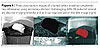
DualBeam
DualBeam systems combine the imaging and analysis capabilities of SEM with the sample modification capabilities of FIB. Cross sectional analysis in a DualBeam provides access to subsurface information that is otherwise inaccessible for SEM imaging. In a DualBeam, the ion and electron beams intersect at a 52° angle. In operation, the sample is positioned normal to the ion beam with its surface at the beam intersection. In this configuration the face of a cross section cut by the ion beam is simultaneously exposed to the electron beam for high-resolution imaging. Live cross-sectional imaging ensures that the process can be halted when the targeted feature is revealed, and before it is destroyed.A “Slice & View” technique takes three-dimensional imaging to the next level. It cuts a sequence of cross sections through the sample at designated intervals, automatically acquiring and saving an image of each section. The stack of images is then reconstructed into a virtual model of the sample. The model can be rotated to any viewing angle, virtually resectioned, and rendered with surfaces that follow contrast contours to emphasize structural details.
FIB can also deposit material with nanoscale control. In the deposition process, a volatile precursor material is introduced through a fine needle in the vicinity of the beam and sample surface. The beam decomposes the precursor into a nonvolatile component that deposits on the surface and a volatile component that is pumped away by the vacuum system. A variety of materials are available, including metals and insulators. The same kind of injector system can be used to introduce gases that enhance FIB milling speed.
FIB should not be neglected as an imaging technique in its own right. FIB images are particularly sensitive to channeling effects and are very useful for visualizing grain structures.
SEM Applications in Failure Analysis
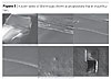
In the following example, SEM is used to find a defect in an automotive paint sample. The sample is a model car, of course, but it does illustrate the versatility of the sample chamber and stage. The defect is cross sectioned, imaged and its elemental composition is determined (Figure 2).Figure 3 shows a zoom series of SEM images that are shot at progressively higher magnifications. The low magnification image at upper left demonstrates the large field of view and excellent depth of field available. The series zooms in on a defect. The image at the lower right was shot at a magnification of 4000x. In it the defect has been cross sectioned by the ion beam and the sample retilted to show the wedge shaped FIB pit from above. The rectangular feature on top of the defect is a protective layer about 2 microns thick deposited by the FIB prior to cross sectioning to protect any delicate surface structure from erosion by the “tails” of the ion beam during the milling process.
Figure 4 shows three images that are a secondary electron SEM image (left), a FIB-induced secondary electron image (middle) and an X-ray map overlaid on the SEM image. The defect appears to be a particle inclusion. The FIB-deposited protective layer overlays the particle. The bright, “liquid” appearance of the particle in the left image is an artifact of charging. The variations in contrast among the grains in the lower layer of the middle image show the sensitivity of FIB images to grain orientation due to channeling effects. The X-ray map overlaid in the right image was set to display Ca in red and Si in green. The composition of the inclusion often helps to identify the source.
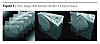
In Figure 5 we see three images that illustrate the Slice & View technique. The system automatically cuts a sequence of cross sections through the region of interest and acquires a high-resolution image of each one. The image stack (left) is combined to reconstruct a three-dimensional model (middle) of the region. The model can be rotated, resectioned and rendered to reveal internal structure.
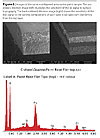
Figure 6 contains images of the same multilayer automotive paint sample. The secondary electron image on the left illustrates the sensitivity of the SE signal to surface topography. The backscattered electron image in the middle shows the sensitivity of the BSE signal to the varying composition of each layer. Both images were acquired in low vacuum conditions, the SE image with a large field gaseous detector (ESEM) and the BSE with a solid state detector, and show no charging despite the insulating nature of the sample. The X-ray spectrum (bottom) was acquired from the top layer. The energy levels (x-axis) of the spectral peaks indicate the elemental identity of the emitting atoms. A quantitative determination of the concentration of each element can be derived from the intensity (y-axis) of the peaks.
Conclusion
The latest generation of SEMs provides fast, easy imaging and analysis, even on the wet, dirty, volatile, outgassing, insulating materials that are common in coatings applications. Low-vacuum and extended low-vacuum operation eliminates many of the sample restrictions and much of the sample preparation required for conventional high-vacuum SEM. DualBeam systems that combine SEM and FIB can reveal sub-surface structure, enabling complete three-dimensional modeling and analysis.For further information, contact FEI Electron Optics b.v. Building AAE, Achtseweg Noord 5, P.O. Box 80066, 5600 KA Eindhoven / Acht, The Netherlands, www.FEI.com or William.Neijssen@fei.com; Laurent.Roussel@fei.com.
Looking for a reprint of this article?
From high-res PDFs to custom plaques, order your copy today!


