XPS - A Tool for the Chemical Characterization of Coatings and Interfaces

XPS (X-ray Photoelectron Spectroscopy) is a powerful method for the quantitative chemical characterization of thin films and solid surfaces. In this paper the XPS process and instrumentation will be described briefly, followed by examples that illustrate the power of the technique in the analysis of coated surfaces.
Why is Surface Analysis Necessary?
All solid materials interact with their surroundings via their surfaces. It is therefore crucial that the surface properties of any material are suitable for the proposed application. Modern, high-performance materials will only be suitable for their intended purpose if their surface properties are correctly engineered. Surfaces are very important in a wide range of materials. A few examples are: glasses, painted surfaces, metals, polymers, biomaterials and semiconductor devices.The need for the engineering of surface properties gives rise to the requirement for the detailed chemical characterization of the surface. XPS provides a method for quantitative chemical analysis of surfaces and thin films and consequently is a valuable tool for the surface engineer.
What is XPS?
As the name implies, XPS relies upon Einstein’s photoelectric effect in which an X-ray photon removes an electron from an atom or molecule provided that photon has sufficient energy. The kinetic energy of that electron depends upon the photon energy and the energy required to remove the electron (the binding energy) according to the equation:Binding energy = Photon energy – Kinetic energy
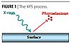
In XPS, the kinetic energy of the emitted electron is measured and so, knowing the photon energy, the binding energy can be calculated. From the binding energy it is possible to determine not only the elemental composition of the surface, but also the chemical state of the elements in the material. The basic XPS process is illustrated in Figure 1.
Why is XPS Surface Specific?
When X-rays strike a solid, they penetrate into the material to a great depth causing photoemission along the whole of their path. However, as the photoelectrons travel through the material, they undergo collisions in which they lose energy. These electrons do not contribute to the peak in the photoelectron spectrum and many do not escape the solid. Only photoelectrons originating close to the surface (within the top 5 to 10 nm, depending on the material) stand a chance of escaping without energy loss. These are the ones than can be detected in the spectrometer.
Components of an XPS Spectrometer
Figure 2 shows a schematic diagram of a modern XPS instrument, the Thermo Scientific K-Alpha. An XPS spectrometer requires a source of X-rays. In modern instruments, an X-ray monochromator delivers Al K-Alpha X-rays to the surface (photon energy = 1486.6 eV). Using this energy it is possible to detect all elements except hydrogen and helium. Non-monochromatic X-ray sources continue to be used, and the photon energy produced by the source is dependent upon the material used for the X-ray anode.


Examples of the Use of XPS in Coatings and Interfaces

There is a range of problems that can affect painted surface production. These include gross faults such as flaking or delamination of the paint film, and more subtle effects such as mottling or crater defects. Failures can occur for a variety of reasons. For example, contamination on the surface prior to coating can result in poor adhesion of the paint film. Alternatively, problems could occur in the coating itself, such as segregation of the components once applied. XPS is a very surface-sensitive technique and the ideal analysis tool for identifying the cause of a particular failure. In this example, the defect under investigation is a crater defect, which appears as a shallow bowl in the film with a raised centre.
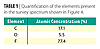
An optical image from XPS system optics is shown in Figure 8 (crater center indicated with an arrow). XPS images of the defect were collected by rastering the stage under the X-ray beam and collecting 128-channel snapshot spectra at each point.
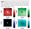

This suggests that the presence of the tin particle not only causes the physical defects (i.e., the crater structure), but also affects the chemistry of the paint film at that location.
Conclusion
XPS is a powerful analytical tool that can provide quantitative, spatially resolved, chemical-state analysis of surfaces and thin films. In this paper it has been shown that quantitative chemical state information can be obtained from coated surfaces. A combination of imaging and small area spectroscopy can be used to establish the nature of features and defects within coatings. Combining XPS spectroscopy with ion beam sputtering provides valuable information about the structure and composition of the film along with the chemistry of the interface region. The K-Alpha represents the latest state-of-the-art XPS spectrometer designed to resolve a wide range of surface and interface materials characterization problems and is uniquely suited for the analysis of coated surfaces.For further information, contact richard.g.white@thermofisher.com.
Looking for a reprint of this article?
From high-res PDFs to custom plaques, order your copy today!