HiPIMS Process Targets Coating of Through-Glass Vias for AI Chips
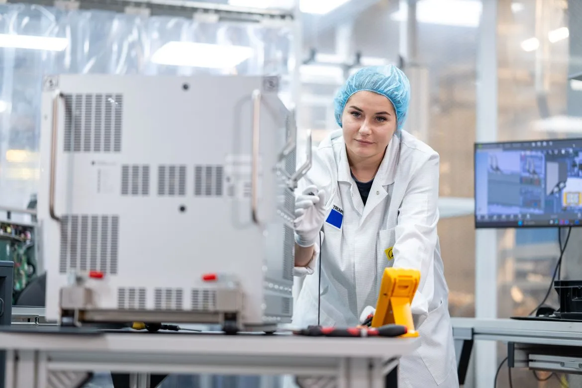
TRUMPF has developed an industrial coating process for through-glass vias used in advanced semiconductor packaging.
Glass substrates can allow chip manufacturers to integrate more functions into smaller spaces and improve data transmission. The substrates require millions of microscopic holes that must be coated with conductive material to create electrical connections.
Even a relatively small number of improperly coated vias can make a glass panel unusable, creating a need for consistent deposition inside structures that are both deep and narrow.
TRUMPF’s HiPIMS generators produce a highly ionized plasma containing a greater proportion of electrically charged particles than conventional methods. Electric and magnetic fields are used to direct those ions into the narrow structures, producing what the company describes as a more uniform coating.
TRUMPF said the process can improve coating quality, process stability and manufacturing yield and help move glass-substrate packaging concepts into series production. The company characterized the technology as the first industrial process of its kind. That designation and the performance comparisons are TRUMPF claims.
The announcement did not identify a customer, commercial production program or individual chip manufacturer using the process.
TRUMPF also supplies ultrashort-pulse lasers used to produce through-glass vias and plasma power systems for semiconductor coating and etching processes.
Learn more about the HiPIMS process for coating through-glass vias.
The process is relevant to PCI readers following manufacturing equipment and precision deposition technologies used in advanced electronics production.
Looking for a reprint of this article?
From high-res PDFs to custom plaques, order your copy today!